Art and Photonics
This page is dedicated to images resulting from experimental measurements in WON, as we believe that some of them are truly mysterious and beautiful and can be used for creating artistic visualizations.
Images resulted by simulation
Experiment by Emadreza Soltanian (Ghent University)
Project: Wideband tunable laser source on a III-V-on-silicon photonic platforms using transfer printing technologies


Multi-Project-Wafer run (MPW)
Experiment by Emadreza Soltanian (Ghent University)
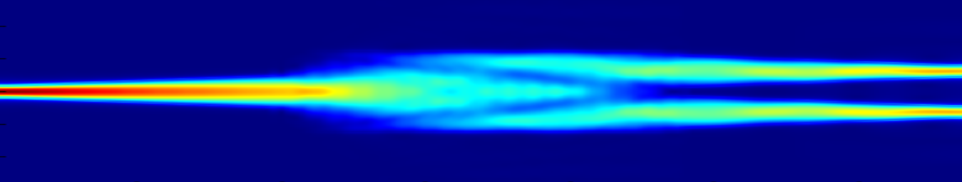
Emadreza was working on a design for a Multi-Project-Wafer run (MPW). He had to simulate every basic component of the optical circuit he intended to design. One of the important passive components of an optical circuit is Multi-Mode-Interferometer (MMI). An MMI 1×2 is able to equally split incoming light into two branches. The interesting fact is that it also is able to combine the light coming from 2 branches into 1.
Geometry parameters of the MMI govern its behaviour over the electromagnetic spectrum. Here is a plot of the splitting behaviour of a 1×2 MMI (E-field plot).

With some artistic effects:

The last image remind us the Eiffel-tower, which was inspired by the skeleton of the human body (thighbone).

E-field plot

